All Categories
History
This section provides an overview for electron microscopes as well as their applications and principles. Also, please take a look at the list of 8 electron microscope manufacturers and their company rankings. Here are the top-ranked electron microscope companies as of July, 2026: 1.TEIJIN LIMITED, 2.Chi Mei Corp., 3.SAMYANG CORPORATION.
Table of Contents
Categories Related to Electron Microscopes
Postdoctoral researcher, conducting research on the production of cathode composite particles for solid-state batteries in the Equipment Engineering Group of Osaka Prefecture University.
Belongs to the Resource and Energy Recycling Laboratory, Nagaoka University of Technology, and conducts research on the development of DDR-type zeolite membranes for CO2 separation and the capture of CO2 from digestion gas generated from sewage treatment plants.
https://researchmap.jp/eiji-hayakawa
Thesis
https://doi.org/10.3390/membranes11080623
http://www.ijcea.org/index.php?m=content&c=index&a=show&catid=109&id=1177
https://www.sciencedirect.com/science/article/abs/pii/S1387181119305529?via%3Dihub
https://www.sciencedirect.com/science/article/abs/pii/S138358661833154X?via%3Dihub
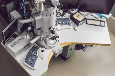
An electron microscope is a microscope that illuminates samples with an electron beam. Due to the extremely short wavelength of the electron beam, it is possible to visualize ultrafine structures that cannot be observed with an optical microscope. There are two main types of electron microscopes: those that output the transmittance of the electron beam as an image, and those that render the signal produced by the interaction between the electron beam and the sample.
Most electron microscopes sold on the market are optimized for industrial materials and for observing biological specimens. The term electron microscope is often abbreviated as “EM.”
In the industrial field, electron microscopes are used to analyze the fractured surface of damaged metal parts to determine the cause of the damage, or to observe the surface of a processed part to check its quality. They are also used to examine the instrumental properties of macromolecular polymers by observing their networks, and to evaluate the presence of impurities. In the life science field, they are used to visualize the microstructure of intracellular organelles and to map the connections between neurons by observing intricately entangled nerve cells. The electron microscope was also awarded the 2017 Nobel Prize in chemistry for its potential application in the structural analysis of proteins by performing simple pretreatments on samples.
Electron microscopes comprise a source, a lens, and a detector, and have a configuration very similar to that of an optical microscope. However, each of these elements is very different in principle from that of an optical microscope.
First of all, electron beams are immediately attenuated and annihilated when they collide with molecules and other substances in the air. Therefore, electron beams must be generated and emitted in a vacuum.
Second, since glass lenses such as those used in general optical systems are transparent, magnetic lenses that converge by applying a magnetic field must be used to refract the electron beams.
Such lenses have large optical aberrations, so they are designed with a small numerical aperture to mitigate this issue. This allows electron microscopes to have a deep depth of focus and to observe objects in three dimensions with great depth.
Standard electron microscopes are classified into two categories:
In these microscopes, an electron beam is transmitted through the sample, and contrast is obtained based on its attenuation. The sample must be very thin for the electron beam to be able to penetrate it. The strength of the electron beam is called the acceleration voltage. At an acceleration voltage of 300 kV, the wavelength is 0.00197 nm, which is extremely short, and the resolution is 0.1 nm, which is on the order of the size of the original material. The resolution is 0.1 nm, which is on the order of the size of the original material. This is 800,000 times higher than the resolution of an optical microscope. Transmission electron microscopes are excellent for observing the internal structure of a sample, such as a crystalline structure in a very compact area, because they observe the electrons transmitted through the sample.
When materials are illuminated with electron beams in a vacuum, secondary electrons, reflected electrons, and characteristic X-rays are emitted. Scanning electron microscope images are formed from secondary electrons and reflected electron signals by scanning a spatially focused electron beam. Secondary electrons are generated near the surface of the specimen, making the secondary electron image suitable for viewing microscopic irregularities in the specimen. The number of reflected electrons depends on the composition of the sample (atomic number, crystal orientation, etc.), making the reflected electron image suitable for evaluating the compositional distribution of the sample surface.
When an electron beam strikes a sample, the atoms that make up the surface are excited and emit electrons. Other emissions include reflected electrons and characteristic X-rays, which are called secondary electrons, and are obtained by point-scanning the intensity of the emitted secondary electrons.
Electron microscopes have extremely high resolution compared to ordinary optical microscopes, facilitating, for example, the observation of microscopic tissue structures such as cells and metal crystals on the order of atomic size.
Taking cells as an example, optical microscopes cannot observe in detail the minute structures other than the nucleus, but electron microscopes can. This makes it possible to investigate in detail the function of enzymes in the cell, reactions of cellular structures, and various other functions.
*Including some distributors, etc.
Sort by Features
Sort by Area

Thermo Fisher Scientific Inc., founded in 1956 and headquartered in Waltham, Massachusetts, is a manufacturer and supplier of life science solutions, analytical instruments, specialty diagnostics, laboratory products, and biopharma services. Through its brand names, including Invitrogen, Fisher Scientific, Patheon, Applied Biosystems, and Gibco, among others, the company provides a wide range of products, which include chromatography systems, thermal cyclers, automated cell counters, fermenters, and DNA polymerases. The company’s annual revenue is over 40 billion USD, and it serves several fields, including customers working in clinical diagnostic labs, research institutions, hospitals, government agencies, and pharmaceutical/biotech companies.
Hitachi High Tech was established in April 1947 and operates in 26 countries with products and services ranging from semiconductor manufacturing equipment and Medical and Biosystems to Analytical Systems and Manufacturing related equipment and solutions. A unique state-of-the-art technology company with two functions as a manufacturer and a trading company with the motto of "Tackling social issues," the Hitachi High-Tech Group aspires to be a company that pursues not only economic value, such as revenue and profit, but also provides social and environmental value by contributing to resolving social issues through its business activities, including products and services. They also provide one-stop services, such as evaluations and analysis at a global level.

Jenoptik was established in 1991 and is based in Jena, Germany, as a manufacturer of optical technologies with majority of their products and services being provided to the photonics market. The company's products portfolio includes imaging solutions and cameras, laser and laser technology, optics and optical systems, and LiDAR technologies, which are mainly used in industries such as, semiconductor and equipment manufacturing, automotive, medical technology, security and defense technology, and aviation.
ZEISS Microscopy, established in Jena, Germany, in 1846 is a manufacturer of optics and optoelectronics used in Precision Mechanics, Binoculars, Microscopy, and Eyeglass Lenses. Their product portfolio includes precision optics, such as lenses, mirrors, and prisms, laser mirrors used in laser cutting, and medical devices, optoelectronic devices and Coatings and Thin Films. The company also provides solutions including industrial quality, microscopy research, project simulation, sample testing and product development. The company also offers customer services that include support, custom research projects and customized services.

JEOL Ltd. is a Japanese developer and manufacturer of scientific and industrial equipment originally established in 1949 as Japan Electron Optics Laboratory Co., Ltd. before its rebrand to JEOL Ltd. in 1961. Based in Akishima, Tokyo, the company produces various spectrometers, electron microscopes, electron beam lithography systems (EBLs), and thin-film formation equipment (TFFE). They also manufacture equipment for clinical testing or analysis, such as clinical chemistry analyzers and rack handlers. JEOL has operations and subsidiaries in three continents, including JEOL (Europe) B.V., JEOL USA Inc. and JEOL (UK) Ltd.
Hitachi High-Tech Analytical Science, established in 1947, is a manufacturer of analytical solutions such as analyzers, handheld thickness gauges, calorimeters, mobile & stationary spectrometers, and elemental analysis products used in environmental screening, general chemicals, metal finishing, metal production, and PMI inspection. The company offers consumables and accessories such as springs for electrodes, mineral oil, x-ray warning lamp bulbs, electrode brush, tungsten electrode, and sample films. The Westford, MA, company offers customized support packages, warranties, preventative maintenance & recertification, consultation services, and rental equipment.
TEIJIN LIMITED, founded in Chiyoda-ku, Tokyo, in 1918 is a manufacturer of aramid, carbon fibers & composites, films, resins & plastics. The company's product portfolio includes polycarbonate (PC) resin, polyphenylene sulfide (PPS) resin, and molded parts and Pharmaceutical & Medical Equipment. Their products are used in industries such as Food and Beverage Processing, Pharmaceutical and Biotechnology and Chemical and Petrochemical and construction. The company also provides services including national distribution, product selection, customized services, technical support and customer service.

Samyang Corporation is a South Korean manufacturer and distributor of a diverse range of products, including petrochemicals, food ingredients, and packaging material such as ethylene, propylene, and butadiene, food ingredients like high-fructose corn syrup and maltodextrin, and packaging materials including PE films and PVC films. Established in 1924, their products are in pharmaceuticals, food additives, and industrial chemicals. The company is particularly known for its development of premium quality pharmaceutical ingredients and is a excellent supplier of such ingredients to the global pharmaceutical industry. Won 2021 Korea Green Management Grand Prize for excellent environmental management performance.
Ranking as of July 2026
Derivation Method| Rank | Company | Click Share |
|---|---|---|
| 1 | TEIJIN LIMITED |
29.6%
|
| 2 | Chi Mei Corp. |
15.4%
|
| 3 | SAMYANG CORPORATION |
12.6%
|
| 4 | ZEISS Microscopy |
10.3%
|
| 5 | Thermo Fisher Scientific Inc. |
8.1%
|
| 6 | JENOPTIK AG |
6.2%
|
| 7 | JEOL Ltd. |
6.1%
|
| 8 | Hitachi High-Tech America, Inc. |
5.9%
|
| 9 | Hitachi High-Tech Analytical Science |
5.8%
|
Derivation Method
The ranking is calculated based on the click share within the electron microscope page as of July 2026. Click share is defined as the total number of clicks for all companies during the period divided by the number of clicks for each company.Number of Employees
Newly Established Company
Company with a History
*Including some distributors, etc.
*Including some distributors, etc.
| Country | Number of Companies | Share (%) |
|---|---|---|
|
United States of America
|
2 | 33.3% |
|
Germany
|
1 | 16.7% |
| Deutschland | 1 | 16.7% |
|
Japan
|
1 | 16.7% |
|
Republic of Korea
|
1 | 16.7% |
41 products found
41 products

Hokkai Photoelectronics Co., Ltd.
630+ people viewing
Photoelectron microscope MyPEEM ■Observe photoelectrons emitted from the sample surface ・Two-dimensional mapping of electronic states on solid sur...

Asmec Co., Ltd.
480+ people viewing
Last viewed: 1 day ago
Solectrix GmbH was founded in Germany in 2005 by founders Lars Helbig and Stefan Schütz. We comprehensively design and support the development of c...

Meishin Koki Co., Ltd.
1370+ people viewing
Last viewed: 2 hours ago
■Summary ・Quickly confirm shapes and compositions that cannot be seen with an optical microscope alone ・Desktop SEM equipped with various functio...

360+ people viewing
Last viewed: 1 hour ago
■SEC “Tabletop SEM (SNE-4500M Plus B)” Although it is a desktop SEM, it is a high-end model with performance comparable to general-purpose SEMs. Th...

JEOL Ltd.
890+ people viewing
Last viewed: 4 hours ago
■Automatic Observation and Analysis Function "Neo Action" Intuitive operation allows anyone to easily automate SEM observation and EDS analysis. ■...

JEOL Ltd.
1380+ people viewing
Last viewed: 1 day ago
■ New Sample Preparation Solution The JIB-PS500i offers three solutions to assist in TEM sample preparation. It enables a reliable and high-through...

Meishin Koki Co., Ltd.
2480+ people viewing
Last viewed: 18 hours ago
■Summary ・General-purpose SEM equipped with FE electron gun ・Automated functions have also evolved, greatly improving the overall capabilities of...

Cosmo Trading Co., Ltd.
930+ people viewing
Last viewed: 3 hours ago
■Development background and main features Tabletop scanning electron microscopes are being used in a variety of fields, mainly electrical equipment...

JEOL Ltd.
960+ people viewing
Last viewed: 10 hours ago
The JEM-ACE200F is an electron microscope compatible with systems that allow operators to acquire data without directly operating the electron micr...

Cosmo Trading Co., Ltd.
870+ people viewing
Last viewed: 1 day ago
The JEOL InTouchScope™ series features three features that transform your analyzer into a tool. JSM-IT200 is a cost-effective scanning electron mi...

Unisoku Co., Ltd.
810+ people viewing
UNISOKU has formed a technical partnership with France's Orsay Physics to provide high spatial resolution FIB/SEM columns that are compatible with ...

JEOL Ltd.
900+ people viewing
Last viewed: 2 hours ago
■Features ・Background and Main Features Benchtop scanning electron microscopes are increasingly being used in various fields, primarily in electri...

Cosmo Trading Co., Ltd.
950+ people viewing
Simple SEM ■Simply select the field of view you want to photograph Simple SEM supports daily routine work. ■Put the sample in and observe without ...
4 models listed

Cosmo Trading Co., Ltd.
760+ people viewing
■SEM used every day. So it's easy to use. Observation objects are becoming smaller day by day as technology advances. The JSM-IT700HR was born from...

Ryokosha Co., Ltd.
730+ people viewing
Last viewed: 1 day ago
■Summary A system that allows high-resolution observation and analysis with the same operability as a tungsten SEM. ■Features ・Equipped with Zero...

JEOL Ltd.
860+ people viewing
Last viewed: 10 hours ago
■ Towards a more accessible tool for everyone Transmission electron microscopes (TEMs) with an acceleration voltage of 120 kV are widely used in th...

Cosmo Trading Co., Ltd.
1420+ people viewing
Last viewed: 20 hours ago
The JSM-IT800 is equipped with an "in-lens Schottky Plus field emission electron gun" to achieve high-resolution observation, a next-generation ele...
5 models listed

Ryokosha Co., Ltd.
590+ people viewing
Last viewed: 1 day ago
■Summary Equipped with the functions of the top-of-the-line tungsten SEM model JSM-IT500, this compact device is equipped with new functions that m...

Cosmo Trading Co., Ltd.
870+ people viewing
■Easy access to the data you need JSM-IT210 is JEOL's most compact stationary scanning electron microscope. The newly developed stage has all 5 axe...

Cosmo Trading Co., Ltd.
860+ people viewing
Last viewed: 1 day ago
Nowadays, not only resolution and analysis performance on the nanometer order, but also throughput when acquiring data is important, so the newly c...

Ryokosha Co., Ltd.
570+ people viewing
Last viewed: 4 hours ago
■Summary Top model of tungsten SEM. Equipped with new functions that make observation work more efficient, the device becomes easier to use. ■Feat...

Ryokosha Co., Ltd.
890+ people viewing
■Features ・JCM-7000 is a tabletop scanning electron microscope with the concept that "anyone can operate SEM/EDS". ・“Zeromag” allows you to obser...
