All Categories
History


This section provides an overview for transmission electron microscopes as well as their applications and principles. Also, please take a look at the list of 8 transmission electron microscope manufacturers and their company rankings. Here are the top-ranked transmission electron microscope companies as of April, 2026: 1.Nanoscience Instruments, 2.Lasertec Corporation, 3.Toray Research Center, Inc..
Table of Contents
Categories Related to Transmission Electron Microscopes
A transmission electron microscope (TEM) is a measurement device that can observe the internal structure of a sample.
It is a type of electron microscope that observes the inside of an ultra-thin sample by irradiating electron beams onto the sample and detecting the transmitted and scattered electrons that pass through the sample. The technique is used in various fields, including materials engineering and biochemistry, as it enables the observation of the internal structure of a sample at a high magnification, which is not feasible with an optical microscope.

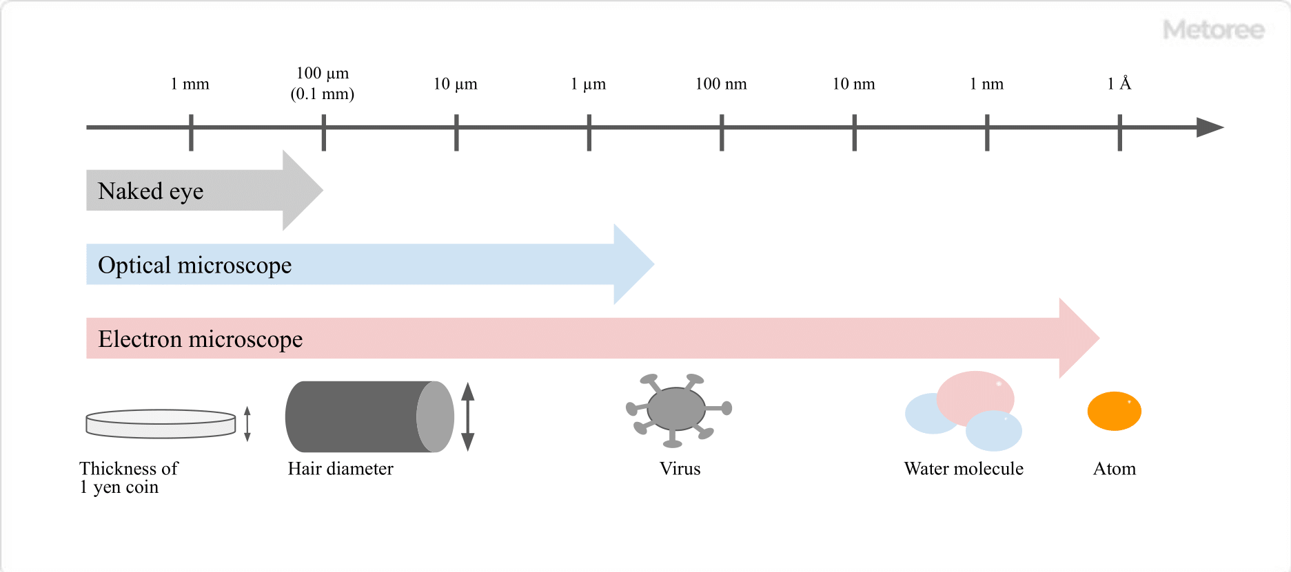
Figure 1. Types and resolutions of microscopes
TEMs are used to observe the internal structure of a sample at magnifications of several hundred to several million times.
It is possible to observe entire cells at the level of tens of micrometers, as well as atomic structures of atomic arrangements at the level of a few Å (1Å (angstrom) = 10-10m). It finds application in the structural analysis of diverse materials, such as semiconductors and ceramics, as well as in the structural analysis of biological samples like cells and bacteria. Various information can be obtained, such as observation of electron diffraction patterns by adjusting the lens system, and elemental analysis and state analysis by attaching an additional spectrometer. Unlike scanning transmission electron microscopes (STEM), TEMs are sometimes used to observe changes in the structure of an object over time, since image data can be acquired at once.

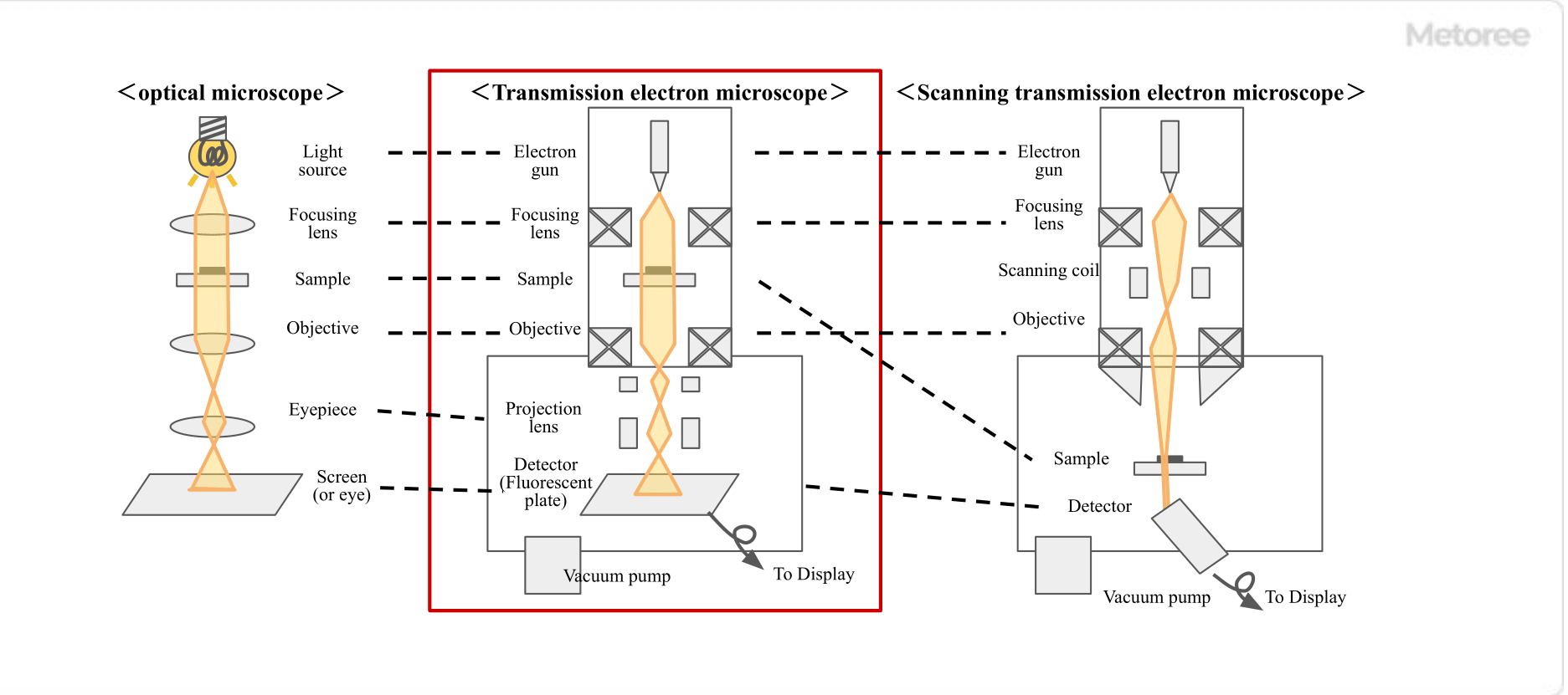
Figure 2. Types of microscopes and structural images
The principle of TEMs is to irradiate a sample with accelerated electrons and observe its internal state by detecting the electrons transmitted through the sample. The structure of the microscope is similar to that of an optical microscope. However, since the light source is an electron beam rather than visible light, the thickness of the sample must be reduced to a level where electrons can penetrate (100 nm or less). The difference in the density of electrons transmitted through the sample appears as a contrast.
The shorter the wavelength of the electrons irradiating the sample (the higher the energy), the higher the resolution (~0.1nm), since the wavelength of electrons accelerated at an acceleration voltage of 300kV is 0.00197nm, which is much shorter than the wavelength of visible light (about 380nm to 780nm) used in optical microscopy.
The higher the acceleration voltage, the shorter the wavelength and the higher the resolution. However, this increases the damage to the sample and must be adjusted appropriately. The upper limit of resolution is about 50pm due to factors such as aberration of the optical system.
Some samples require appropriate sample preparation.
Thick Specimens
Samples to be observed by general transmission electron microscopes need to be thinned to a thickness of about 100nm.
1. Dispersion Method
The sample is dispersed in a solvent, and the dispersion is dropped onto a substrate for observation.
2. Microtome Method
This method uses a diamond knife to thin the sample to about 100nm. Soft samples such as polymers are cooled with liquid nitrogen and then cut.
3. Ar Milling Method
A sample that has been mechanically thinned to a thickness of several tens of micrometers is irradiated with Ar+ ions, which breaks the bonds in the sample while thinning it.
4. FIB Method
The target area is thinned by FIB while observing with a scanning electron microscope (SEM). Using an ultra-high voltage electron microscope (HVEM) with an acceleration voltage of 1000kV or higher, it is possible to observe samples with a thickness of about 5µm. However, since the equipment is very large and the structure of the microscope is complex, it is mainly owned by research facilities such as universities.
Samples That Do Not Contain Heavy Elements
Polymer and biological samples are mainly composed of light elements such as C, H, N, and O, which are highly permeable to electrons and may not provide sufficient contrast to identify the Structure of the sample. Selective electron staining with a staining agent with high electron scattering capacity (e.g., OsO4 or RuO4) in the area where the structure of the sample is to be observed will provide an image with sufficient contrast. Electron staining can alter the Structure of the sample. To avoid this effect, it is effective to use the phase contrast method of transmission electron microscopy or scanning transmission electron microscopy (STEM).
Samples That Evaporate or Sublimate Under High Vacuum Conditions
Evaporation or sublimation under high vacuum conditions not only changes the Structure of the sample and its shape but can also lead to equipment failure. To prevent this, environmentally controlled transmission electron microscopes (ETEM) or cryo-electron microscopes should be used.

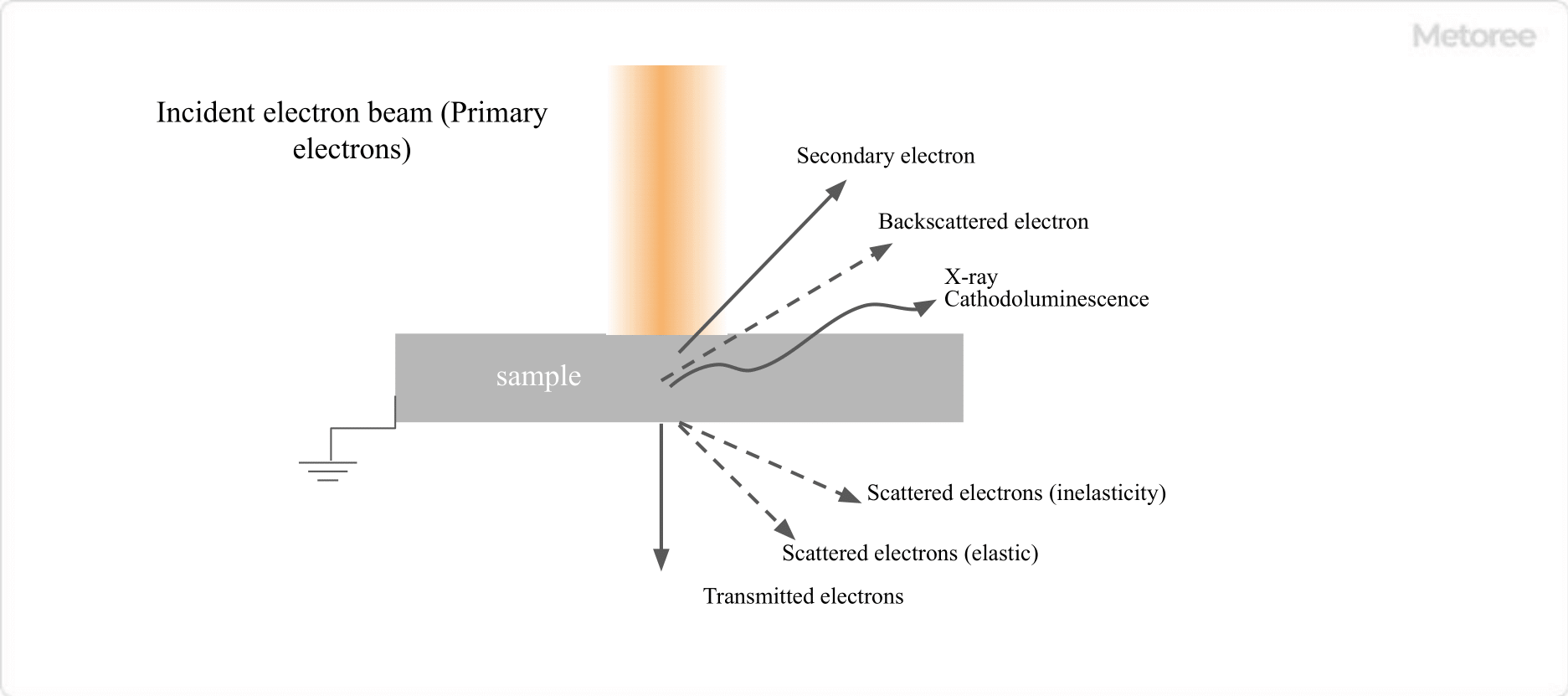
Figure 3. Main electromagnetic waves generated by electron beam irradiation
Since various signals other than electrons can be obtained by irradiating a sample with an accelerated electron beam, transmission electron microscopes may be equipped with various types of analytical instruments.
Electron Beam Diffraction
By detecting the interference of elastically scattered electron beams, a diffraction image of the sample is obtained. Analysis of the diffraction image reveals crystallographic information, such as the Structure of the crystal and its orientation.
Electron Energy Loss Spectroscopy (EELS)
Inelastically scattered electron beams are those emitted from a sample after the incident electron beam excites electrons in the sample. By measuring how much energy is lost by the electron beam compared to before the incident beam, information about the composition and bonding state of the sample can be determined.
Electron Tomography
By applying the principles of CT (computer tomography) to transmitted electrons, we can produce a three-dimensional stereoscopic image of a sample by stacking cross-sectional images of the sample.
Various other analytical functions can be added to these. Compared to measurements made with an independent measuring device, more detailed measurements can be made because the measurement position can be selected while viewing the transmission electron microscope image.
*Including some distributors, etc.
Sort by Features
Sort by Area

Nanoscience Instruments is a manufacturer and supplier of nanoscience instruments that was established in 2002 and is headquartered in Oak Ridge, Tennessee, USA. The company produces a wide range of instruments, including atomic force microscopes, scanning electron microscopes, and transmission electron microscopes. Its products such as Desktop Scanning Electron Microscopes, Ion Mills, Electrospinners & Electrosprayers, Optical & Force Tensiometers and Battery Cyclers are used by a number of researchers in academia, pharmaceutical, and biotechnology industries. The company also provides a range of services, including custom manufacturing, sem solutions, nanomaterial fabrication, surface and interfacial analysis, TEM solutions and support.

Hitachi High Tech was established in April 1947 and operates in 26 countries with products and services ranging from semiconductor manufacturing equipment and Medical and Biosystems to Analytical Systems and Manufacturing related equipment and solutions. A unique state-of-the-art technology company with two functions as a manufacturer and a trading company with the motto of "Tackling social issues," the Hitachi High-Tech Group aspires to be a company that pursues not only economic value, such as revenue and profit, but also provides social and environmental value by contributing to resolving social issues through its business activities, including products and services. They also provide one-stop services, such as evaluations and analysis at a global level.

JEOL Ltd. is a Japanese developer and manufacturer of scientific and industrial equipment originally established in 1949 as Japan Electron Optics Laboratory Co., Ltd. before its rebrand to JEOL Ltd. in 1961. Based in Akishima, Tokyo, the company produces various spectrometers, electron microscopes, electron beam lithography systems (EBLs), and thin-film formation equipment (TFFE). They also manufacture equipment for clinical testing or analysis, such as clinical chemistry analyzers and rack handlers. JEOL has operations and subsidiaries in three continents, including JEOL (Europe) B.V., JEOL USA Inc. and JEOL (UK) Ltd.

JEOL Ltd, founded in 1949 and located in Tokyo, Japan, is a manufacturer of metrology instruments, industrial equipment, and medical equipment. The company offers a diverse product catalog, including electron microscopes for semiconductor inspection, electron beam metal additive manufacturing machines, and electron spin resonance spectrometers. These products find applications in various fields, including analyzing impurities in solvents for semiconductor fabrication, conducting differential analysis of chocolates with different cacao content, and analyzing bimetallic complexes, among other applications.

Lasertec Corporation, founded in 1960 and headquartered in Yokohama, Japan, is a manufacturer and supplier of semiconductor-related systems, FPD-related systems, and laser microscopes. The company's product portfolio includes mask inspection systems, mask edge inspection systems, FPD photomask inspection systems, laser microscopes, and lithium-ion batteries. These products find applications in various sectors, including materials science, the flat panel display industry, semiconductor manufacturing, biomedical and life sciences, as well as research and development. The company is ISO 45001 and ISO 9001 certified, with offices in the USA, China, Singapore, Taiwan, and South Korea for global outreach.


The Max Planck Institute for Marine Microbiology was founded in 1992 and is a researcher and supplier of products and services to the scientific community, headquartered in Bremen, Germany. The institute specializes in research related to the diversity and function of marine microorganisms, interactions in the marine environment, and the impact of climate change. It provides access to research laboratories, specialized equipment, and educational and training programs. MPIMM is a part of the Max Planck Society and caters to the general public, academic research, biotechnology, pharmaceutical, and energy industries.
Ranking as of April 2026
Derivation Method| Rank | Company | Click Share |
|---|---|---|
| 1 | Nanoscience Instruments |
27.7%
|
| 2 | Lasertec Corporation |
14.7%
|
| 3 | Toray Research Center, Inc. |
12.0%
|
| 4 | Hitachi High-Tech America, Inc. |
10.6%
|
| 5 | TRI-GENOTOUL |
10.3%
|
| 6 | AnaPath Services GmbH |
9.9%
|
| 7 | JEOL Ltd. |
6.8%
|
| 8 | The Max Planck Institute for Marine Microbiology |
5.2%
|
| 9 | JEOL Ltd |
2.9%
|
Derivation Method
The ranking is calculated based on the click share within the transmission electron microscope page as of April 2026. Click share is defined as the total number of clicks for all companies during the period divided by the number of clicks for each company.Number of Employees
Newly Established Company
Company with a History
*Including some distributors, etc.
*Including some distributors, etc.
| Country | Number of Companies | Share (%) |
|---|---|---|
 United States of America
|
2 | 50.0% |
 Japan
Japan
|
1 | 25.0% |
 Germany
|
1 | 25.0% |
43 products found
43 products
Bruker Corporation
470+ people viewing
Last viewed: 5 hours ago
■Electron microscope built-in system Bruker's electron microscope built-in nanoindentation system (Picoindenter) can be incorporated into an SEM/TE...
4 models listed
Bionet Research Institute Co., Ltd.
520+ people viewing
Last viewed: 1 day ago
BesTEM is software that performs simulation calculations of high-resolution TEM/STEM images using the multi-slice method. In recent years, aberrati...
Irie Co., Ltd.
590+ people viewing
Last viewed: 7 hours ago
■Features ・Excellent performance, multi-function, and overwhelmingly low price. Excellent cost performance. ・1.2 nm image resolution (when using ...
Meishin Koki Co., Ltd.
1210+ people viewing
Last viewed: 1 day ago
■Summary ・Quickly confirm shapes and compositions that cannot be seen with an optical microscope alone ・Desktop SEM equipped with various functio...
Solutions Systems Co., Ltd.
960+ people viewing
Last viewed: 1 day ago
■ Overview Simulate a grid statue, a high -resolution photo of a transmitted electron microscope, with a multi -slice method. If you enter various ...
JEOL Ltd.
760+ people viewing
Last viewed: 1 day ago
■Automatic observation and analysis function "Neo Action" With intuitive operation, anyone can easily automate SEM observation and EDS analysis. ■...
Bionet Research Institute Co., Ltd.
340+ people viewing
Last viewed: 1 day ago
We help with image analysis of TEM/SEM, STEM, cryo-TEM, etc. Realize work efficiency.
3 models listed
JEOL Ltd.
1220+ people viewing
Last viewed: 4 hours ago
◾️ New sample preparation solution JIB-PS500i provides three solutions to assist in TEM sample preparation. From sample preparation to TEM observa...
Irie Co., Ltd.
490+ people viewing
Last viewed: 21 hours ago
■Five imaging modes in one unit ・Equipped with TEM, STEM, SEM, EDS, and ED modes -Easy switching of imaging modes with intuitive software ・Bright...
Meishin Koki Co., Ltd.
2000+ people viewing
Last viewed: 3 hours ago
■Summary ・General-purpose SEM equipped with FE electron gun ・Automated functions have also evolved, greatly improving the overall capabilities of...
Cosmo Trading Co., Ltd.
830+ people viewing
Last viewed: 1 day ago
■Development background and main features Tabletop scanning electron microscopes are being used in a variety of fields, mainly electrical equipment...
JEOL Ltd.
820+ people viewing
Last viewed: 1 day ago
The JEM-ACE200F is an electron microscope compatible with a system that allows operators to acquire data without directly operating the electron mi...
Solutions Systems Co., Ltd.
450+ people viewing
Last viewed: 1 day ago
■ Characteristics ・ Create a 3D surface stereos (Digital Elevation Map) from SEM with a deep depth or an optical camera stereo or three images. ・...
2 models listed
Cosmo Trading Co., Ltd.
770+ people viewing
Last viewed: 1 day ago
The JEOL InTouchScope™ series features three features that transform your analyzer into a tool. JSM-IT200 is a cost-effective scanning electron mi...
Unisoku Co., Ltd.
710+ people viewing
Last viewed: 1 day ago
UNISOKU has formed a technical partnership with France's Orsay Physics to provide high spatial resolution FIB/SEM columns that are compatible with ...
JEOL Ltd.
800+ people viewing
Last viewed: 1 day ago
◾️Features ・Development background and main features Tabletop scanning electron microscopes are being used in a variety of fields, mainly electri...
Solutions Systems Co., Ltd.
800+ people viewing
Last viewed: 18 hours ago
■ Overview DISS 5 is a device and software that digitizes the system by retrofitting an existing analog SEM device. It is an active system that can...
Cosmo Trading Co., Ltd.
560+ people viewing
Last viewed: 1 day ago
Simple SEM ■Simply select the field of view you want to photograph Simple SEM supports daily routine work. ■Put the sample in and observe without ...
4 models listed
Cosmo Trading Co., Ltd.
660+ people viewing
Last viewed: 1 day ago
■SEM used every day. So it's easy to use. Observation objects are becoming smaller day by day as technology advances. The JSM-IT700HR was born from...
JEOL Ltd.
750+ people viewing
Last viewed: 1 day ago
◾️ A more familiar tool for everyone Transmission electron microscopes (TEM) with an accelerating voltage of 120 kV are widely used in the field o...
Cosmo Trading Co., Ltd.
700+ people viewing
Last viewed: 1 day ago
The JSM-IT800 is equipped with an "in-lens Schottky Plus field emission electron gun" to achieve high-resolution observation, a next-generation ele...
5 models listed
Cosmo Trading Co., Ltd.
790+ people viewing
Last viewed: 1 day ago
■Easy access to the data you need JSM-IT210 is JEOL's most compact stationary scanning electron microscope. The newly developed stage has all 5 axe...
Cosmo Trading Co., Ltd.
750+ people viewing
Last viewed: 1 day ago
Nowadays, not only resolution and analysis performance on the nanometer order, but also throughput when acquiring data is important, so the newly c...
Oxford Instruments Ltd.
410+ people viewing
Last viewed: 1 day ago
Relate is a correlation software package optimized for working with electron microscopy, EDS, EBSD, and AFM data and images. It provides the tools ...
Musashino Denshi, INC.
460+ people viewing
Last viewed: 1 day ago
This is a mechanical polishing device for preparing thin specimens for transmission electron microscopy (TEM). Ideal when using an ion milling devi...
Hulinks Co., Ltd.
270+ people viewing
Last viewed: 8 hours ago
■Main functions of CrystalKit CrystalKit is a program that allows you to construct various types of crystal defects such as point defects, grain bo...
Hulinks Co., Ltd.
300+ people viewing
Last viewed: 1 day ago
Tempas" implements HRTEM (high-resolution transmission electron microscopy) image/diffraction simulation functions, as well as STEM (scanning trans...