All Categories
History


This section provides an overview for scanning electron microscopes (sem) as well as their applications and principles. Also, please take a look at the list of 10 scanning electron microscope (sem) manufacturers and their company rankings. Here are the top-ranked scanning electron microscope (sem) companies as of April, 2026: 1.Schaefer SEE Srl, 2.Nanoscience Instruments, 3.Electron Optics Instruments, LLC..
Table of Contents
Categories Related to Scanning Electron Microscopes (SEM)

A SEM (scanning electron microscope) is a type of electron microscope that allows us to observe the surface conditions of a sample by irradiating the sample with electron beams and detecting the secondary electrons emitted from the sample.
A SEM makes it possible to observe even minute structures that are difficult to observe with an optical microscope. For this reason, it is used in a wide range of fields, such as materials engineering and biochemistry.

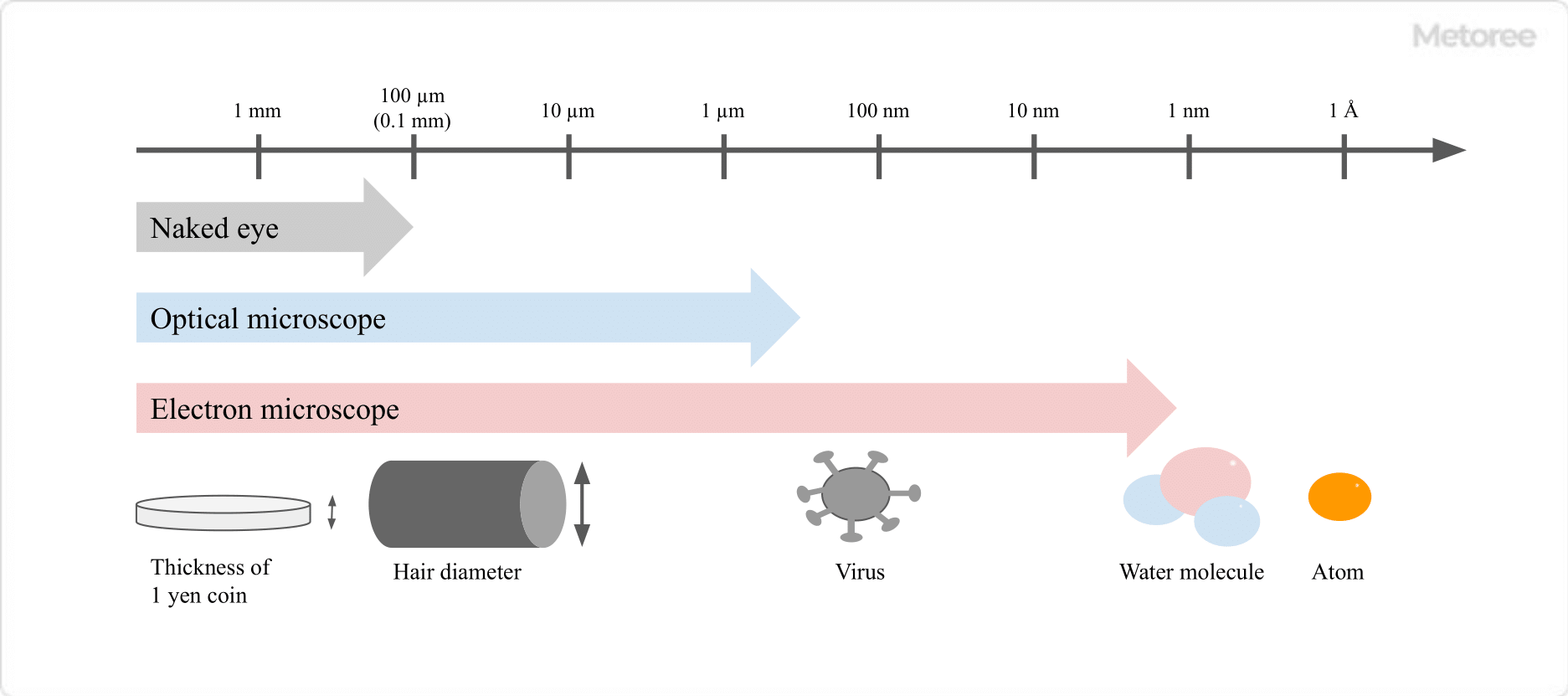
Figure 1. Types and resolutions of microscopes
The magnification of SEMs can be increased to several hundred thousand times, and the resolution can be increased to several nm. It also has features such as a deep depth of focus that make it easy to observe unevenness in the sample.
The magnification limit of an optical microscope is about 1,000x and the resolution limit is about 150nm.
In addition, unlike images obtained with optical microscopes, SEMs provide three-dimensional images with contrast, in which the plane perpendicular to the direction of incidence of the electron beam is darker and the closer the plane is to parallel, the brighter the image becomes.
Taking advantage of these features, SEMs are used to observe the surface conditions of various materials, such as semiconductor and ceramic materials, microorganisms such as bacteria and viruses, and biological samples such as cells. On the other hand, transmission electron microscopes are generally used to observe the internal structure of samples.

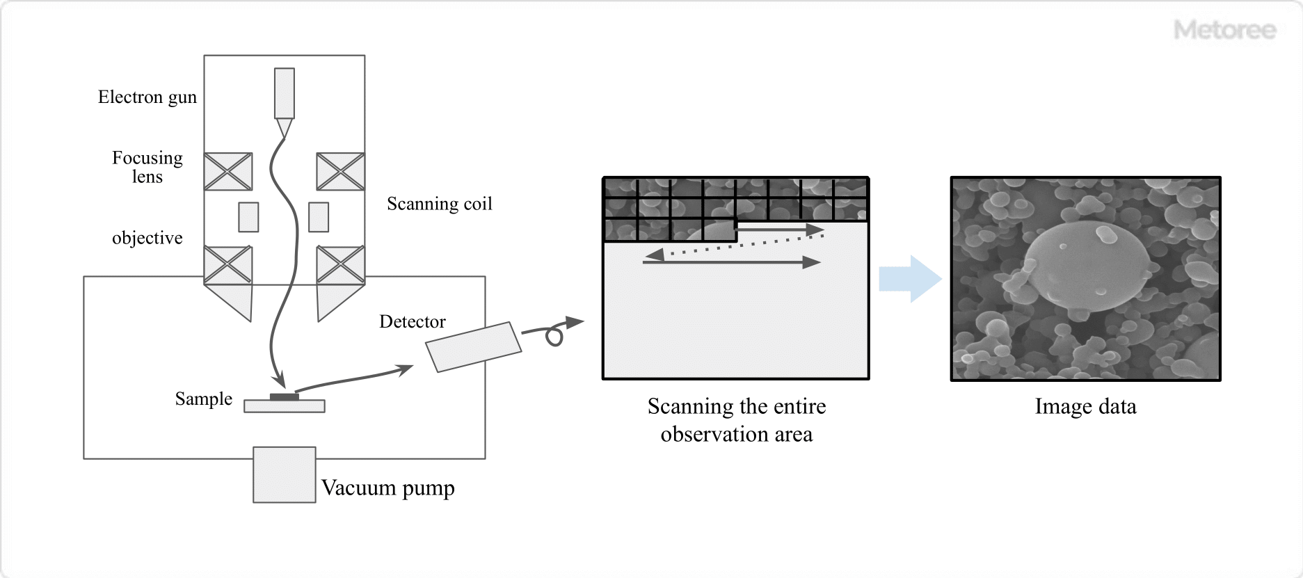
Figure 2. Structure and measurement image of scanning electron microscope
In SEMs, an accelerated electron beam is focused on the surface of a sample and irradiated, and the secondary electrons (SE) and backscattered electrons (BSE) generated during the irradiation are detected and analyzed.
By increasing the acceleration voltage and irradiating electron energy, the resolution can be increased to a few nm. Increasing the acceleration voltage increases the resolution. However, too high an acceleration voltage can cause problems such as the influence of reflected electrons from deeper positions in the sample and charging. Therefore, acceleration voltages of several kV to several tens of kV are usually used.
Secondary electrons are electrons ejected from near the surface of the sample when an electron beam is applied.
The state of the electrons differs according to the unevenness of the sample, creating contrast in the image data obtained by measuring secondary electrons and allowing observation of surface irregularities and particle shapes.
Backscattered electrons, on the other hand, are electrons that are bounced back when an electron beam interacts with an atom.
The reflectance of the emitted electrons differs depending on the atom. By measuring backscattered electrons, the contrast is enhanced for each type of atom and the distribution of atoms in the sample can be observed.
SEMs mainly consist of an electron gun that emits electron beams, an electron lens that focuses the electron beams onto the sample surface, and a detector that detects secondary electrons and backscattered electrons.
There are three types of electron guns: thermal electron emission, field emission, and Schottky type, each with different characteristics. Electron lenses are generally of the type in which an electric current is passed through a coil and the electron beam is controlled by a magnetic field, and there are various types, such as the out-lens type and in-lens type.
The inside of SEMs are kept in a high vacuum of about 10^-4 Pa during measurement. In recent times, however, some SEMs have been developed that can measure under low vacuum (about 10^2 Pa) or atmospheric pressure, and are often used in the biological field where samples with high moisture content are used.
SEMs can be used to measure a wide variety of samples, but some samples require appropriate sample preparation and measurement conditions.
Insulating Specimens
When using an insulating sample, the surface of the sample may be charged by the irradiated electron beam. This can cause image distortion and anomalous contrast, which may result in inaccurate image data. To prevent charging, it is necessary to take measures such as coating the sample surface with a thin sputtering of metal, observing at a low acceleration voltage, and observing under low vacuum conditions.
Samples That Evaporate or Sublimate under High Vacuum Conditions
If evaporation or sublimation occurs under high vacuum conditions, it not only changes the structure or shape of the sample but may also lead to equipment failure. To prevent these problems, it is effective to take measures, such as measuring under low vacuum conditions. In addition, biological samples that contain a lot of water often require separate pretreatment even for observation in a low vacuum.
Magnetic Samples
When using magnetic samples, if the distance between the electron lens and the sample is too close, the sample may become magnetized, making it difficult to adjust the electron beam, and large samples may come off the sample stand and be absorbed by the lens. To prevent these problems, it is necessary to use SEMs with an out-lens system or similar, and fix the specimen with screws or adhesives.
To Observe the Inside of a Sample
If you want to observe the inside of a sample without using the transmission mode described below, you need to process the sample using a focused ion beam (FIB) or the like and observe the cross-section.

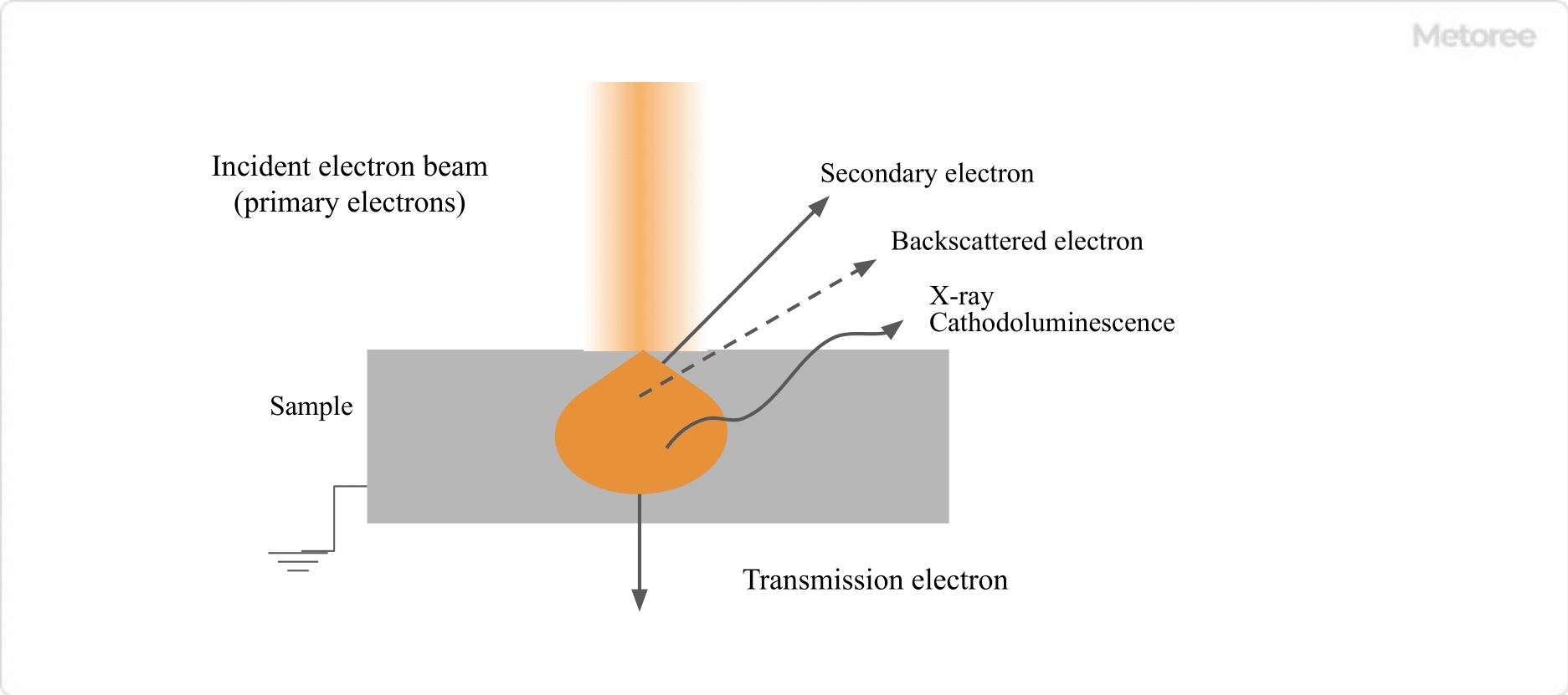
Figure 3. Example of electromagnetic waves emitted by electron beam irradiation
When a sample is irradiated with an accelerated electron beam, signals such as transmission electrons, X-rays, cathodoluminescence, and absorbed electrons as well as secondary electrons and backscattered electrons can be obtained. Analyzers may be attached to detect these signals.
Transmitted Electrons
If the thickness of the sample is thin enough or if the material is particulate, a portion of the irradiated electrons will be transmitted through the sample and can be detected as transmitted electrons. Generally, transmission electrons are measured by a transmission electron microscope or a scanning transmission electron microscope (STEM), which are independent measurement devices. Scanning transmission electron microscope (STEM) It is possible to observe internal structures that SEMs are not good at.
X-ray
When an atom is irradiated by an electron beam, X-rays are sometimes emitted in addition to electron beams. Since each atom has its own unique energy, it is possible to identify the type of atoms present on the sample surface by detecting the emitted X-rays.
There are two types of X-ray detectors: energy-dispersive X-ray detectors (EDS) and wavelength-dispersive X-ray detectors (WDS). Each has different characteristics and should be selected according to the purpose.
Cathodoluminescence
Cathodoluminescence is the light emitted when a sample is irradiated by an electron beam. By detecting this light, it is possible to measure the crystal properties of the sample, such as crystal defects, impurities, and carrier concentration.
Various other functions can be added by adding other options. Compared to the case where measurement is performed by an independent measurement device, the SEMs have the advantage that the measurement position can be selected while viewing the SEM's image, allowing for more detailed measurement.
*Including some distributors, etc.
Sort by Features
Sort by Area

Nanoscience Instruments is a manufacturer and supplier of nanoscience instruments that was established in 2002 and is headquartered in Oak Ridge, Tennessee, USA. The company produces a wide range of instruments, including atomic force microscopes, scanning electron microscopes, and transmission electron microscopes. Its products such as Desktop Scanning Electron Microscopes, Ion Mills, Electrospinners & Electrosprayers, Optical & Force Tensiometers and Battery Cyclers are used by a number of researchers in academia, pharmaceutical, and biotechnology industries. The company also provides a range of services, including custom manufacturing, sem solutions, nanomaterial fabrication, surface and interfacial analysis, TEM solutions and support.

Thermo Fisher Scientific Inc., founded in 1956 and headquartered in Waltham, Massachusetts, is a manufacturer and supplier of life science solutions, analytical instruments, specialty diagnostics, laboratory products, and biopharma services. Through its brand names, including Invitrogen, Fisher Scientific, Patheon, Applied Biosystems, and Gibco, among others, the company provides a wide range of products, which include chromatography systems, thermal cyclers, automated cell counters, fermenters, and DNA polymerases. The company’s annual revenue is over 40 billion USD, and it serves several fields, including customers working in clinical diagnostic labs, research institutions, hospitals, government agencies, and pharmaceutical/biotech companies.

Hitachi High Tech was established in April 1947 and operates in 26 countries with products and services ranging from semiconductor manufacturing equipment and Medical and Biosystems to Analytical Systems and Manufacturing related equipment and solutions. A unique state-of-the-art technology company with two functions as a manufacturer and a trading company with the motto of "Tackling social issues," the Hitachi High-Tech Group aspires to be a company that pursues not only economic value, such as revenue and profit, but also provides social and environmental value by contributing to resolving social issues through its business activities, including products and services. They also provide one-stop services, such as evaluations and analysis at a global level.


TESCAN, established in 1991 with headquarters in the Czech Republic, is a manufacturer of SEM (scanning electron microscopes). The company's products include gallium ion and xenon ion plasma FIB SEM, 4D-STEM (scanning transmission electron microscopy) systems, and micro-CT 3D and 4D scanners. The company's products are used to facilitate image acquisition, reconstruction, visualization, quantification, and analysis of microscopic samples in the materials science, life sciences, earth sciences, and semiconductor markets among others.

JEOL Ltd. is a Japanese developer and manufacturer of scientific and industrial equipment originally established in 1949 as Japan Electron Optics Laboratory Co., Ltd. before its rebrand to JEOL Ltd. in 1961. Based in Akishima, Tokyo, the company produces various spectrometers, electron microscopes, electron beam lithography systems (EBLs), and thin-film formation equipment (TFFE). They also manufacture equipment for clinical testing or analysis, such as clinical chemistry analyzers and rack handlers. JEOL has operations and subsidiaries in three continents, including JEOL (Europe) B.V., JEOL USA Inc. and JEOL (UK) Ltd.

ZEISS Microscopy, established in Jena, Germany, in 1846 is a manufacturer of optics and optoelectronics used in Precision Mechanics, Binoculars, Microscopy, and Eyeglass Lenses. Their product portfolio includes precision optics, such as lenses, mirrors, and prisms, laser mirrors used in laser cutting, and medical devices, optoelectronic devices and Coatings and Thin Films. The company also provides solutions including industrial quality, microscopy research, project simulation, sample testing and product development. The company also offers customer services that include support, custom research projects and customized services.

Schaefer SEE SRL, founded in 2005 with headquarters in Italy, is a distributor of nanoscale measuring and imaging equipment and accessories. The company's product line includes SPM microscopes for operation in air environments and vacuums, tabletop SEM microscopes, optical 3D digital microscopes, and 3D/4D label-free microscopes. These products are used for research and development in various industries, including medicine, water treatment, solar power, cosmetics, and pharmaceuticals. The company carries brands that include Advanced Diamond Technologies, AppNano, Oxford Instruments, IZON Science, and OCI Vacuum Microengineering.

ATA Scientific Pty. Ltd., established in 1990 with headquarters in Australia, is a distributor and supplier of scientific instruments and laboratory equipment. The company's products include lab-scale, air-driven, high-pressure homogenizers, the CellBox portable CO2 incubator, the Quantum Tx single bacterial cell counter, protein analyzers, and the Zetasizer Ultra, used for the measurement of particles and molecular size, particle charge, and particle concentration. The company serves scientific and research laboratories in the education, food processing, manufacturing, pharmaceutical, and chemical processing markets.

McCrone Associates Inc., established in 1956 with headquarters in the USA, has expanded into The McCrone Group and is a provider of materials analysis and education and a distributor of digital imaging systems, microscope accessories, and laboratory supplies. The McCrone Group includes McCrone Associates, Inc.; McCrone Microscopes & Accessories, LLC; Hooke College of Applied Sciences, LLC; and ModernMicroscopy.com. The company's products include Nikon light microscopes, Linkam heating and cooling stages, the JEOL NeoScope benchtop SEM, and Timegate spectroscopy instruments. These products are used for microscopy, microanalysis, and material characterization by scientific and research laboratories.
Ranking as of April 2026
Derivation Method| Rank | Company | Click Share |
|---|---|---|
| 1 | Schaefer SEE Srl |
20.8%
|
| 2 | Nanoscience Instruments |
18.8%
|
| 3 | TESCAN |
9.3%
|
| 4 | Electron Optics Instruments, LLC. |
9.3%
|
| 5 | ZEISS Microscopy |
7.7%
|
| 6 | McCrone |
7.1%
|
| 7 | Hitachi High-Tech America, Inc. |
6.9%
|
| 8 | Thermo Fisher Scientific Inc. |
6.4%
|
| 9 | ATA Scientific Pty Ltd. |
5.5%
|
| 10 | JEOL Ltd. |
4.7%
|
Derivation Method
The ranking is calculated based on the click share within the scanning electron microscope (sem) page as of April 2026. Click share is defined as the total number of clicks for all companies during the period divided by the number of clicks for each company.Number of Employees
Newly Established Company
Company with a History
*Including some distributors, etc.
*Including some distributors, etc.
| Country | Number of Companies | Share (%) |
|---|---|---|
 United States of America
|
3 | 33.3% |
 Japan
Japan
|
2 | 22.2% |
 Czech Republic
|
1 | 11.1% |
| Deutschland | 1 | 11.1% |
 Italy
Italy
|
1 | 11.1% |
 Australia
|
1 | 11.1% |
44 products found
44 products
Asmec Co., Ltd.
410+ people viewing
Last viewed: 1 day ago
Solectrix GmbH was founded in Germany in 2005 by founders Lars Helbig and Stefan Schütz. We comprehensively design and support the development of c...
Meishin Koki Co., Ltd.
1210+ people viewing
Last viewed: 59 minutes ago
■Summary ・Quickly confirm shapes and compositions that cannot be seen with an optical microscope alone ・Desktop SEM equipped with various functio...
290+ people viewing
■SEC “Tabletop SEM (SNE-4500M Plus B)” Although it is a desktop SEM, it is a high-end model with performance comparable to general-purpose SEMs. Th...
JEOL Ltd.
760+ people viewing
Last viewed: 1 day ago
■Automatic observation and analysis function "Neo Action" With intuitive operation, anyone can easily automate SEM observation and EDS analysis. ■...
Meishin Koki Co., Ltd.
2000+ people viewing
Last viewed: 6 hours ago
■Summary ・General-purpose SEM equipped with FE electron gun ・Automated functions have also evolved, greatly improving the overall capabilities of...
Cosmo Trading Co., Ltd.
830+ people viewing
Last viewed: 1 day ago
■Development background and main features Tabletop scanning electron microscopes are being used in a variety of fields, mainly electrical equipment...
Cosmo Trading Co., Ltd.
770+ people viewing
Last viewed: 59 minutes ago
The JEOL InTouchScope™ series features three features that transform your analyzer into a tool. JSM-IT200 is a cost-effective scanning electron mi...
Unisoku Co., Ltd.
710+ people viewing
Last viewed: 59 minutes ago
UNISOKU has formed a technical partnership with France's Orsay Physics to provide high spatial resolution FIB/SEM columns that are compatible with ...
JEOL Ltd.
800+ people viewing
Last viewed: 1 day ago
◾️Features ・Development background and main features Tabletop scanning electron microscopes are being used in a variety of fields, mainly electri...
Cosmo Trading Co., Ltd.
560+ people viewing
Last viewed: 1 day ago
Simple SEM ■Simply select the field of view you want to photograph Simple SEM supports daily routine work. ■Put the sample in and observe without ...
4 models listed
Unisoku Co., Ltd.
900+ people viewing
Last viewed: 1 day ago
The world's first new single-molecule imaging method. Achieving subnanometer-scale Raman spectroscopic imaging by improving the S/N ratio and sensi...
Cosmo Trading Co., Ltd.
660+ people viewing
Last viewed: 1 day ago
■SEM used every day. So it's easy to use. Observation objects are becoming smaller day by day as technology advances. The JSM-IT700HR was born from...
Ryokosha Co., Ltd.
610+ people viewing
Last viewed: 1 day ago
■Summary A system that allows high-resolution observation and analysis with the same operability as a tungsten SEM. ■Features ・Equipped with Zero...
Cosmo Trading Co., Ltd.
700+ people viewing
Last viewed: 1 day ago
The JSM-IT800 is equipped with an "in-lens Schottky Plus field emission electron gun" to achieve high-resolution observation, a next-generation ele...
5 models listed
Unisoku Co., Ltd.
700+ people viewing
Last viewed: 1 day ago
Achieves atomic resolution STM of 6K or less using a mechanical refrigerator, allowing continuous cooling for long periods of time without using ra...
Ryokosha Co., Ltd.
510+ people viewing
Last viewed: 1 day ago
■Summary Equipped with the functions of the top-of-the-line tungsten SEM model JSM-IT500, this compact device is equipped with new functions that m...
Cosmo Trading Co., Ltd.
790+ people viewing
Last viewed: 1 day ago
■Easy access to the data you need JSM-IT210 is JEOL's most compact stationary scanning electron microscope. The newly developed stage has all 5 axe...
Oxford Instruments Ltd.
1050+ people viewing
Last viewed: 1 day ago
RISE is a revolutionary technology that combines confocal Raman microscopy and SEM. RISE can link structural and chemical composition information o...
Cosmo Trading Co., Ltd.
750+ people viewing
Last viewed: 1 hour ago
Nowadays, not only resolution and analysis performance on the nanometer order, but also throughput when acquiring data is important, so the newly c...
Oxford Instruments Ltd.
2500+ people viewing
Last viewed: 20 hours ago
■Summary The Ultim Extreme Silicon Drift Detector is a breakthrough solution for ultra-high resolution FEG-SEM applications, enabling solutions tha...
Unisoku Co., Ltd.
870+ people viewing
Last viewed: 1 day ago
The most versatile and high-performance multi-probe SPM system on the market, it is a cutting-edge tool for nanotechnology research. This is the wo...
Unisoku Co., Ltd.
850+ people viewing
Last viewed: 1 day ago
Introducing a new middle-end SPM model that is a compact version of the USM1300 and is compatible with low-temperature, high-magnetic fields. This ...
Unisoku Co., Ltd.
1010+ people viewing
Last viewed: 6 hours ago
Highly expandable ultra-high vacuum low temperature SPM, expandable to near-field optical/Raman spectroscopy. This device uses a newly developed cr...
Unisoku Co., Ltd.
990+ people viewing
Last viewed: 1 day ago
High-end model of ultra-low temperature/strong magnetic field STM. It is used both domestically and internationally, contributing to cutting-edge r...
Unisoku Co., Ltd.
1010+ people viewing
Last viewed: 1 day ago
By pre-treating the sample and cleaning the probe in an ultra-high vacuum, STM/AFM can be observed at low temperatures with atomic and molecular le...
Unisoku Co., Ltd.
750+ people viewing
Last viewed: 1 day ago
High-end model of ultra-low temperature, strong magnetic field STM, continuous cooling below 40mK (target 30mK). It is a high-performance STM that ...
Ryokosha Co., Ltd.
480+ people viewing
Last viewed: 1 day ago
■Summary Top model of tungsten SEM. Equipped with new functions that make observation work more efficient, the device becomes easier to use. ■Feat...
Ryokosha Co., Ltd.
760+ people viewing
Last viewed: 1 day ago
■Features ・JCM-7000 is a tabletop scanning electron microscope with the concept that "anyone can operate SEM/EDS". ・“Zeromag” allows you to obser...