All Categories
History
This section provides an overview for semiconductor inspection equipment as well as their applications and principles. Also, please take a look at the list of 5 semiconductor inspection equipment manufacturers and their company rankings. Here are the top-ranked semiconductor inspection equipment companies as of July, 2026: 1.ViSCO Technologies USA, Inc., 2.TAKANO CO.,LTD., 3.JAI.
Table of Contents
Categories Related to Semiconductor inspection equipment
 Semiconductor inspection equipment is equipment that inspects wafers and semiconductor chips for defects in the semiconductor manufacturing process.
The main semiconductor manufacturing processes include the photomask manufacturing process, which is equivalent to a printing plate, the wafer manufacturing process, which is the foundation of semiconductors, the front-end process of forming fine circuit structures on wafers using photomasks, and the back-end process of packaging individual semiconductor chips after circuit formation. If we look at the details, there are hundreds of processes.
In recent years, semiconductor microfabrication technology has reached the nanometer range (about 1/10,000th the thickness of a human hair), and at the same time, wafers have become larger in diameter, so that several thousand semiconductor chips containing billions of transistors can be produced from a single wafer.
Inspection equipment is extremely important in the semiconductor manufacturing process, which boasts such high productivity, leading to early rejection of defective products, cost reduction, and improvement of quality and reliability. The criteria for selecting semiconductor inspection equipment should take into consideration the diameter of the wafer, the process to be used, and the type of defects to be detected.
Semiconductor inspection equipment is used in various phases of the semiconductor manufacturing process.
Defects to be detected using semiconductor inspection equipment include distortion, cracks, scratches, and foreign matter on photomasks and wafers, misalignment of circuit patterns formed in the front-end process, dimensional defects, packaging defects in the back-end process, and many other cases.
For this reason, it is necessary to select appropriate semiconductor inspection equipment and software for each process, and automation using AI, etc. is being promoted to speed up inspections and reduce manpower.
Semiconductor inspection equipment consists of measurement equipment, software to process the measured data, and facilities to perform the appropriate measurement.
High-resolution cameras, electron microscopes, and laser measuring instruments are used as measuring devices. Software for processing the measured data is developed with algorithms that are specific to the process to be inspected. Vibration suppression and lighting equipment are also necessary to ensure proper measurement. The image imaging, image processing, and defect classification technologies that are central to semiconductor inspection equipment are described below.
Wafers are made from semiconductor raw materials such as silicon, which are formed as cylindrical monocrystalline materials called ingots, sliced to a thickness of about 1 mm, and polished on the surface, with a diameter of 12 inches (about 30 cm) these days.
Defects in wafers include not only attached foreign matter but also surface flaws, cracks, uneven processing, and crystal defects on the wafer itself, etc. Detecting these defects mainly by laser beam irradiation is the visual inspection in the wafer manufacturing process.
The front-end process proceeds in the wafer state, and there are two main types of defects that occur there, referred to as random and systematic. Random defects are mainly caused by the presence of foreign matter, but because they are random, their locations are unpredictable. Therefore, random defects on wafers are detected by image processing. Systematic defects, on the other hand, are defects caused by particles adhering to the photomask or exposure process conditions, such as on the photomask, and tend to occur at the same location on each semiconductor chip lined up on the wafer.
In the back-end process, wafers are cut into individual chips (dicing), placed in resin or ceramic packages, and sealed by connecting terminals on the chips to those on the package (wire bonding). The second stage of the process consists mainly of electrical inspections, but also includes visual inspections for wire bonding defects, part number printing defects, etc.
In general, visual inspections in the manufacturing process often aim to check for dirt, scratches, etc., and in some cases have nothing to do with product functionality or performance. However, dirt, scratches, etc. in semiconductor manufacturing are not merely apparent problems; in almost all cases, they are problems that affect functionality and performance.
Semiconductors are electronic devices, and like other electrical and electronic devices, electrical inspections are performed. However, it is extremely difficult to inspect all the billions of transistors and the wiring that connects them, and only visual inspections can confirm things like transistor gates and wiring detail.
In semiconductor processes at the nanometer level, the thickness of a single wire and the spacing between adjacent wires are several nanometers.
If there are nano-order defects here, they can cause wiring shorts or wire breaks. Furthermore, even if the wiring width is 90% of the designed value due to a defect of 1/10th the size, the resistance and capacitance of the wiring will change. When an electric current flows through this wiring, a phenomenon called electromigration, in which metal atoms move due to the movement of electrons, occurs, rapidly thinning the wiring and causing disconnections to occur in a short period.
Thus, semiconductor manufacturing requires visual inspections with extremely fine precision, and as microfabrication technology continues to evolve, the required precision will continue to increase.
*Including some distributors, etc.
Sort by Features
Sort by Area

ViSCO Technologies USA, Inc. is a manufacturer of machine vision systems that was established in March 2014 and is headquartered in Minato-ku, Tokyo, Japan. The company offers a wide range of products, including machine vision cameras, image processing software, and machine vision inspection systems, used in various industries, including automotive, electronics, and food and beverage. ViSCO Technologies also provides machine vision solutions which are known for their quality, dependability, and ease of use. The company is customer-centric, and its products are backed by a comprehensive warranty and support program.

Yasunaga Corporation, founded in 1923 and based in Iga City, Mie Prefecture, Japan, is a manufacturer of engine parts, machine tools, as well as wire saws, and electronics systems. The company's core business are on precision machining of engine components, with connecting rods being a primary product. It has been serving the automotive, semiconductor, and electronic parts industries, delivering machine tools for various processes, including boring, drilling, slicing, assembly, and inspection.
UENO SEIKI CO., LTD., a company founded in March 1972, based in Mizumaki-Cho Onga-gun, Fukuoka, Japan, is a manufacturer of industrial products and equipment that caters to various industries. The company’s product line includes precision machining tools, industrial robots, and automation systems. These equipment are widely used in manufacturing plants for tasks such as cutting, drilling, and assembly. The company also offers customer services, including technical support, product repairs, consultation, and customization to meet the customer's requirements.
JAI is a manufacturer and supplier of digital CMOS camera technolgy designed for industrial machine vision, medical imaging and outdoor applications. The company has branches in Denmark, Germany, Japan, China, Singapore, South Korea, and the USA and distribution partners in more than 35 countries. Additionally, they have sold over 1 million cameras and their Traffic Imaging systems are installed in cities around the globe. Their products are seamlessly integrated into a wide range of processes, products, and services where camera vision technology is used.
Ranking as of July 2026
Derivation Method| Rank | Company | Click Share |
|---|---|---|
| 1 | ViSCO Technologies USA, Inc. |
50.5%
|
| 2 | TAKANO CO.,LTD. |
13.2%
|
| 3 | JAI |
12.1%
|
| 4 | YASUNAGA CORPORATION |
10.7%
|
| 5 | UENO SEIKI CO.,LTD. |
9.1%
|
| 6 | Okano Electric Co., Ltd. |
4.4%
|
Derivation Method
The ranking is calculated based on the click share within the semiconductor inspection equipment page as of July 2026. Click share is defined as the total number of clicks for all companies during the period divided by the number of clicks for each company.Number of Employees
Newly Established Company
Company with a History
*Including some distributors, etc.
*Including some distributors, etc.
| Country | Number of Companies | Share (%) |
|---|---|---|
|
Japan
|
3 | 75.0% |
|
United States of America
|
1 | 25.0% |
45 products found
45 products

Mitani Shoji
1640+ people viewing
Last viewed: 2 hours ago
Cosmofinder is an automatic exterior inspection device made by Mitani Corporation, a professional for image processing and image measurement. The h...
2 models listed
Tokyo Machine Vision System Co., Ltd.
740+ people viewing
Last viewed: 3 hours ago
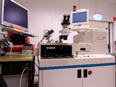
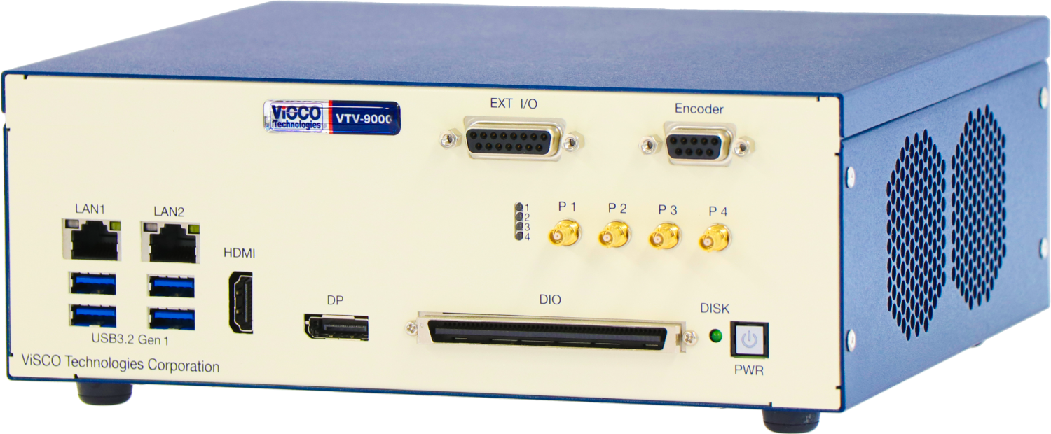
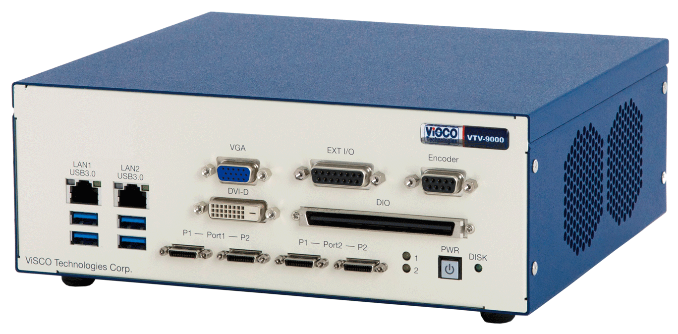
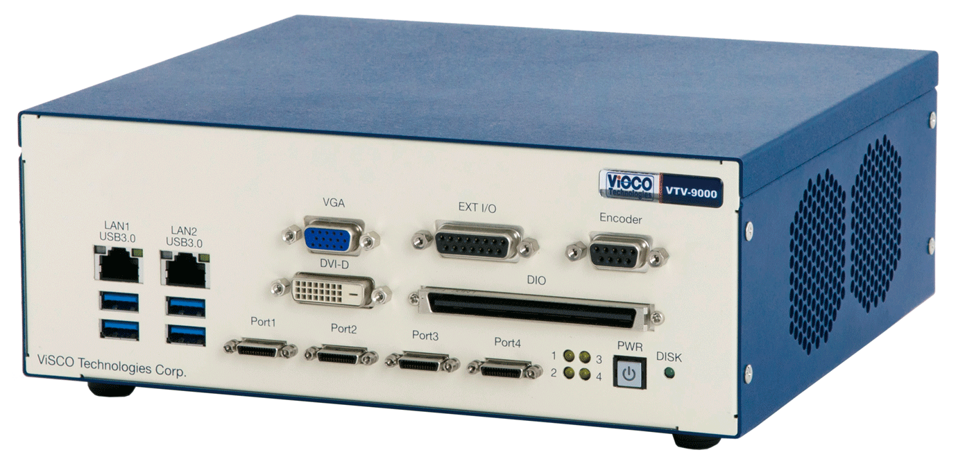
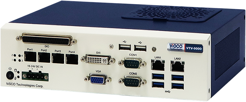
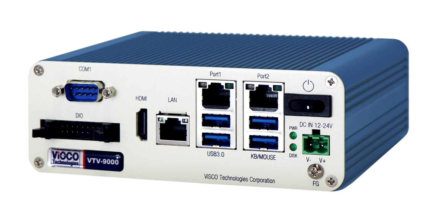
The VTV-9000 series is a software VISIONMANAGER developed by Viscus Technologies and an image processing test that integrates hardware. Intuitive o...
6 models listed

YASUNAGA CORPORATION
390+ people viewing
Last viewed: 2 hours ago
■We propose optimal solutions for automation and labor saving. Yasunaga's machinery equipment business began with processing machines for sewing ma...
2 models listed

JEOL Ltd.
890+ people viewing
Last viewed: 5 hours ago
■Automatic Observation and Analysis Function "Neo Action" Intuitive operation allows anyone to easily automate SEM observation and EDS analysis. ■...

CHUO ELECTRIC WORKS L.T.D
910+ people viewing
The frequency characteristics of wafers are inspected using a vector frequency analyzer on the production line. Multiple voltage output settings ar...

Okano Electric Co., Ltd.
870+ people viewing
Last viewed: 9 hours ago
■Device overview This device is a chip appearance inspection device that uses 6 (4) cameras to inspect the appearance of chip parts supplied from a...

HiSOL,Inc.
850+ people viewing
Last viewed: 1 day ago
The V2000 Brightlight system is easy to use and efficient to inspect various types of defects on wafer surfaces. The system can be operated automat...

Hubrain
1130+ people viewing
Last viewed: 1 day ago
・ This device is a multifunction device that has a both sides of the front and back imaging and the tray stuffing function. ・ Equipped with a high ...

YASUNAGA CORPORATION
900+ people viewing
Last viewed: 2 hours ago
■We propose optimal solutions for automation and labor saving. Yasunaga's machinery equipment business began with processing machines for sewing ma...

JEOL Ltd.
970+ people viewing
Last viewed: 5 hours ago
The JEM-ACE200F is an electron microscope compatible with systems that allow operators to acquire data without directly operating the electron micr...

Okano Electric Co., Ltd.
640+ people viewing
Last viewed: 1 day ago
The surface of the chip component (4th/6th side) is determined by image processing using Okano's proprietary software. Equipment design takes into ...

Nidek Advanced Technology Co., Ltd.
760+ people viewing
■Features ・Realizes simultaneous 3D/2D/SD measurement at high speed and with high accuracy ・Ideal for 3D inspection of gold bumps ・Various conve...

YASUNAGA CORPORATION
820+ people viewing
Last viewed: 2 hours ago
■We propose optimal solutions for automation and labor saving. Yasunaga's machinery equipment business began with processing machines for sewing ma...

Nidek Advanced Technology Co., Ltd.
740+ people viewing
Last viewed: 1 day ago
■Features ・Ultra high speed and high precision inspection ・2D/3D simultaneous measurement system ・Supports finer bump diameter/pitch
Nidek Advanced Technology Co., Ltd.
680+ people viewing
Last viewed: 1 day ago
■Features ・Ultra high speed and high precision inspection ・2D/3D simultaneous measurement system ・Supports finer bump diameter/pitch

YASUNAGA CORPORATION
550+ people viewing
Last viewed: 3 hours ago
■We propose optimal solutions for automation and labor saving. Yasunaga's machinery equipment business began with processing machines for sewing ma...
2 models listed

Nidek Advanced Technology Co., Ltd.
720+ people viewing
Last viewed: 1 day ago
Gold Bump Wafer Process 2D/3D Inspection System High-speed simultaneous height (3D) and appearance (2D) inspection ideal for mass-produced 100% in...
Nidek Advanced Technology Co., Ltd.
640+ people viewing
■Features ・Ultra high speed and high precision inspection ・2D/3D simultaneous measurement system ・Supports finer bump diameter/pitch

Irie Co., Ltd.
1090+ people viewing
Last viewed: 3 hours ago
It is capable of detecting particles on the wafer surface with high sensitivity, and is essential for maintaining yields in semiconductor manufactu...

Irie Co., Ltd.
880+ people viewing
Last viewed: 22 hours ago
Wafer surface equipment WM-10 is suitable for 90-65nm process node, low price and high performance ■Features/Applications ・Achieves maximum detec...