All Categories
History

Product
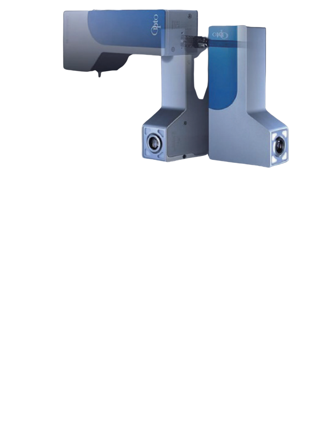
Macro defect inspection device ED-ScopeHandling Company
Photonic Instruments Co., Ltd.Categories
| Image | Part Number | Price (excluding tax) | Weight | Resolution | Observation specifications | Main unit unit configuration | Size | Light source (LED 3W) | Optical field of view | Power supply | Frame rate | PC section unit configuration | ED special image processing | ED processing automatic control mechanism |
|---|---|---|---|---|---|---|---|---|---|---|---|---|---|---|
|
|
ED-Scope |
Available upon quote |
Approximately 30Kg |
5 million pixel CMOS camera (2/3 inch, 2,448 x 2,048 pixels) |
Reflected light (surface defects) / Transmitted light observation (internal defects) |
High-resolution macro lens, digital CMOS camera, special lighting section, micro-tilt sample stage |
300 (W) x 470 (D) x 990 (H) mm |
3W, average lifespan of approximately 25,000h (depending on usage environment), light aperture 0 to 8 levels |
Minimum approximately 136mm (horizontal) x 115mm (vertical) |
AC100V (PC/Monitor) ・AC adapter (light source: DC5V) ・CMOS camera: DC5V:USB3.0 |
35 frames/sec (MAX): Still images (BMP/JPG), videos (MPG) |
PC (windows10), LCD monitor TFT wide 28 inches |
Special image processing software that uses multiple image data |
Automatic motor control and setting of focus mechanism from PC |
Reviews shown here are reviews of companies.
Reviews shown here are reviews of companies.