All Categories
History
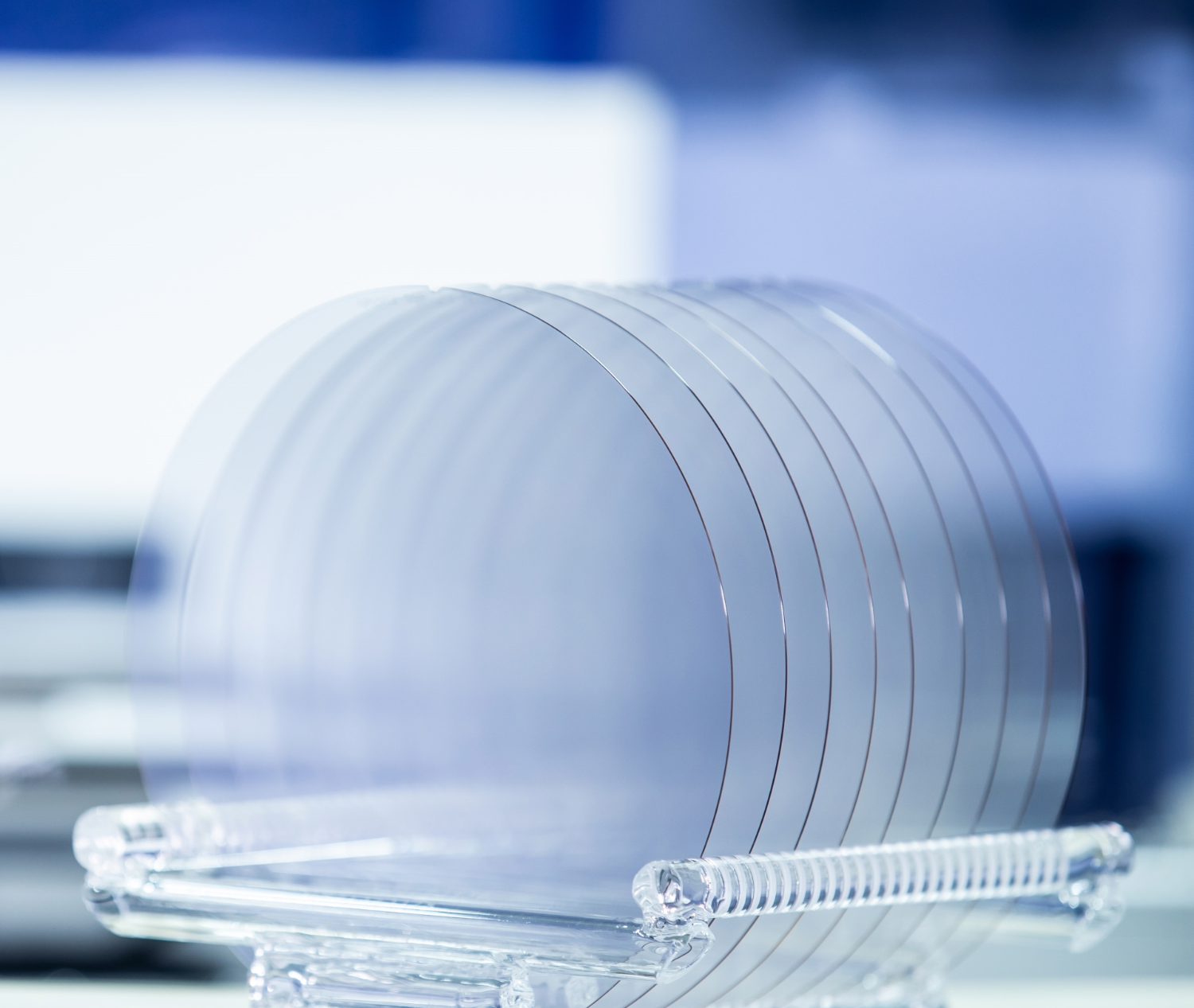
Product
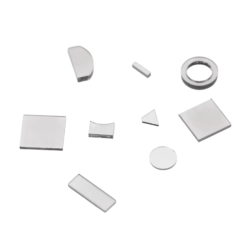
GaN substrate (square)Handling Company
Toyominato Co., Ltd.Categories
| Image | Part Number | Price (excluding tax) | Plane direction | Dislocation density | Effective area | Conductive type | Thickness | Size |
|---|---|---|---|---|---|---|---|---|
|
|
GaN substrate (square) |
Available upon quote |
C-plane (0001) off-angle toward M-axis |
<1 × 10^6 cm-2 |
>90% |
・N-type (Un-doped) |
400 ± 25 µm |
(10 ± 0.5) × (15 ± 0.5) mm2 |
Reviews shown here are reviews of companies.
Reviews shown here are reviews of companies.