All Categories
History
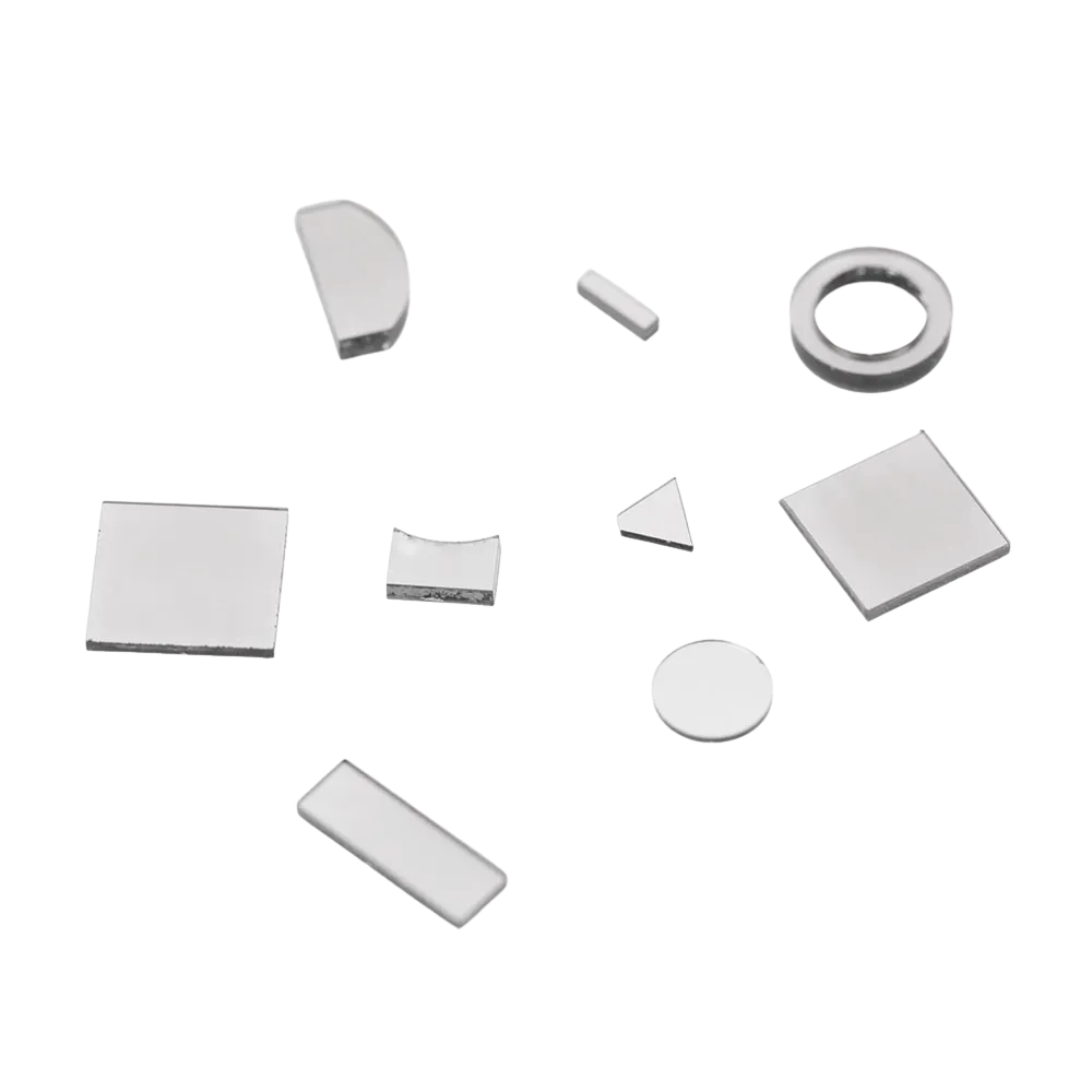
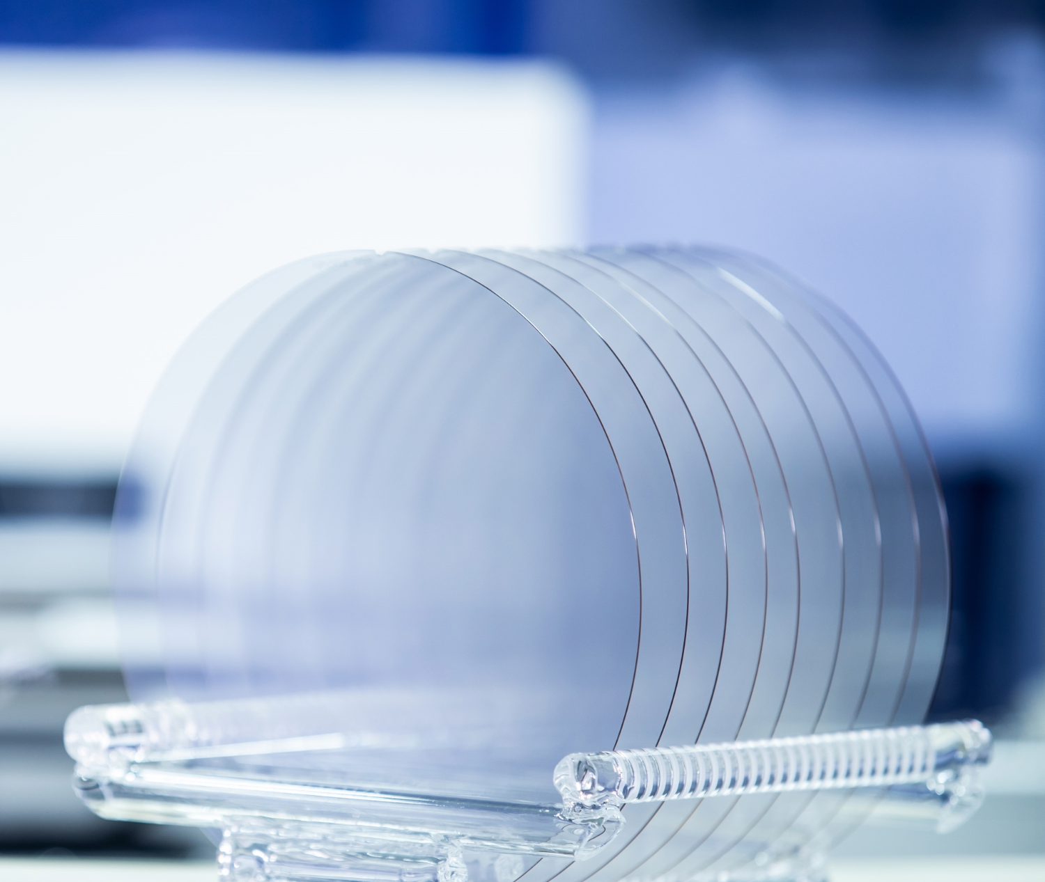
Product
GaN wafer Non-polar GaN square substrate (A side & M side)Handling Company
Toyominato Co., Ltd.Categories
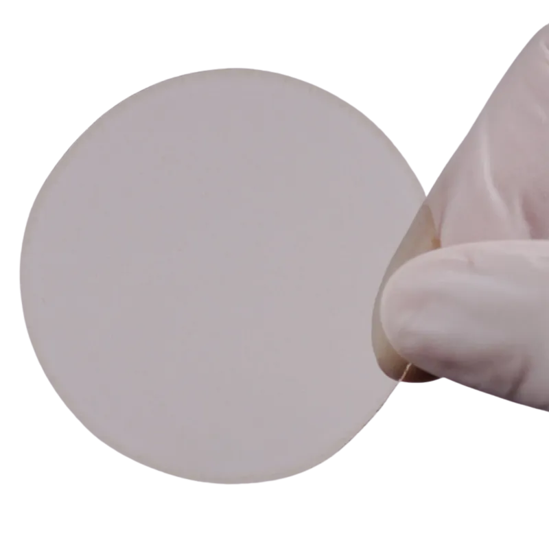
| Image | Part Number | Price (excluding tax) | Electrical resistivity (300K) | Transition defect density | Surface finish | Packing method | Effective area | Azimuth plane | Flatness TTV | Conductive type | Board thickness | Warp BOW | Size | Primary orientation flat orientation. length |
|---|---|---|---|---|---|---|---|---|---|---|---|---|---|---|
|
|
GaN-FS-A-N-S |
Available upon quote |
<0.5Ω・cm |
5×10⁵ pieces/cm2 or less |
Ga side: CMP finish. Ra<0.2nm. Epi-ready finish. |
Filled with nitrogen in a clean room |
90% or more |
A side (1,120) side ±1° |
15um or less |
N type (Undoped) |
350 ±25um |
20um or less |
5mm×10mm, ±0.2mm |
Orientation flat direction (1-100) ± 0.5° |
Reviews shown here are reviews of companies.
Reviews shown here are reviews of companies.